
Helios
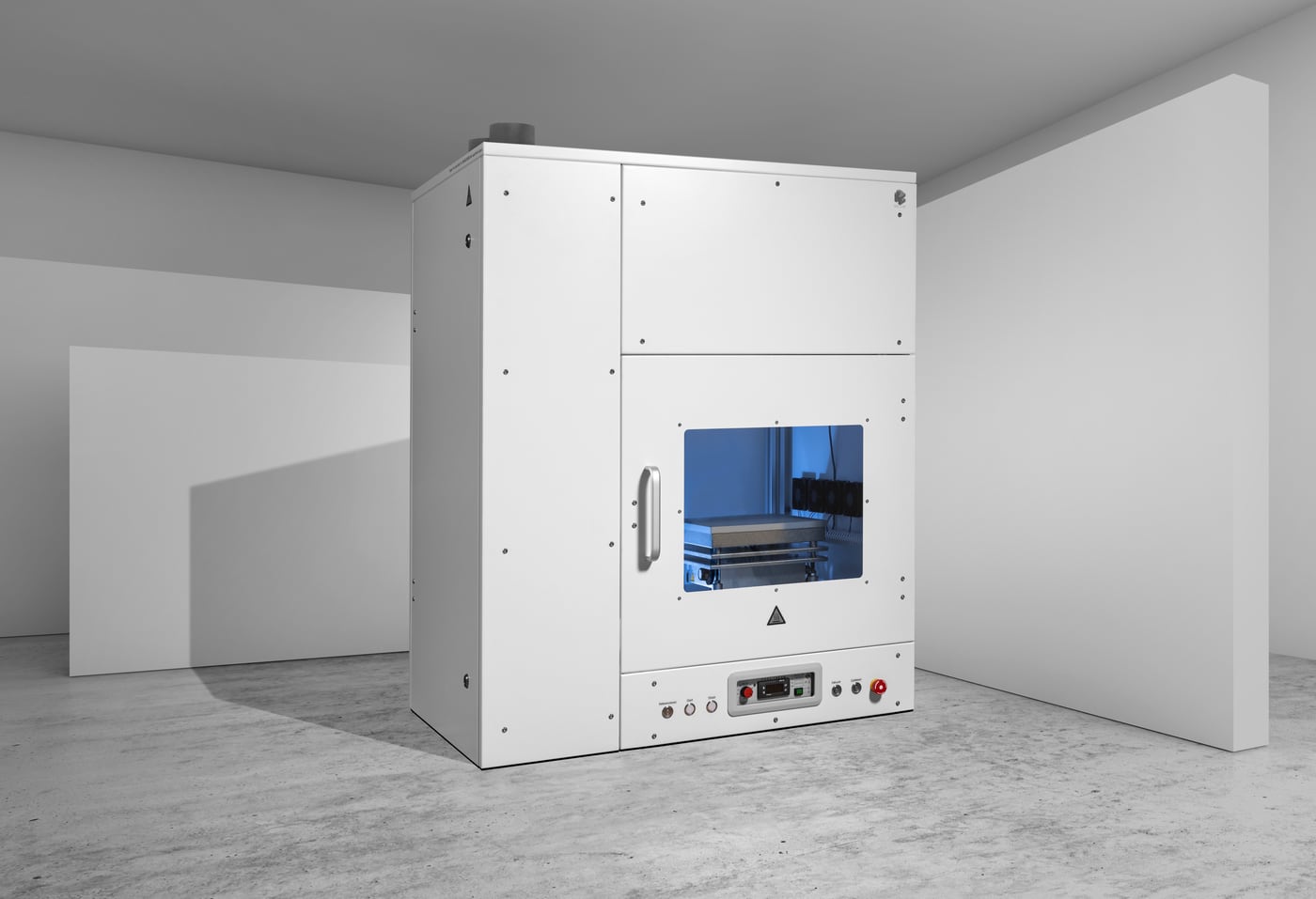
The wafer inspection system: Helios heats, illuminates and measures wafers, making cracks and damage visible.
The later a defect in a wafer shows up, the more expensive it gets. Helios finds cracks and damage before they become a problem: as an inspection and metrology module for quality assurance in semiconductor production. The wafer is held on a hot plate by vacuum and heated under control following a stored recipe, with defined ramp and hold times up to the target temperature.
Then heat, light and software start working together. A dome light projects a fine line pattern through a slit aperture onto the heated wafer, while the linear axis moves it step by step under the camera. Image by image, a complete picture of the surface emerges, in which intelligent object recognition makes cracks and damage visible.
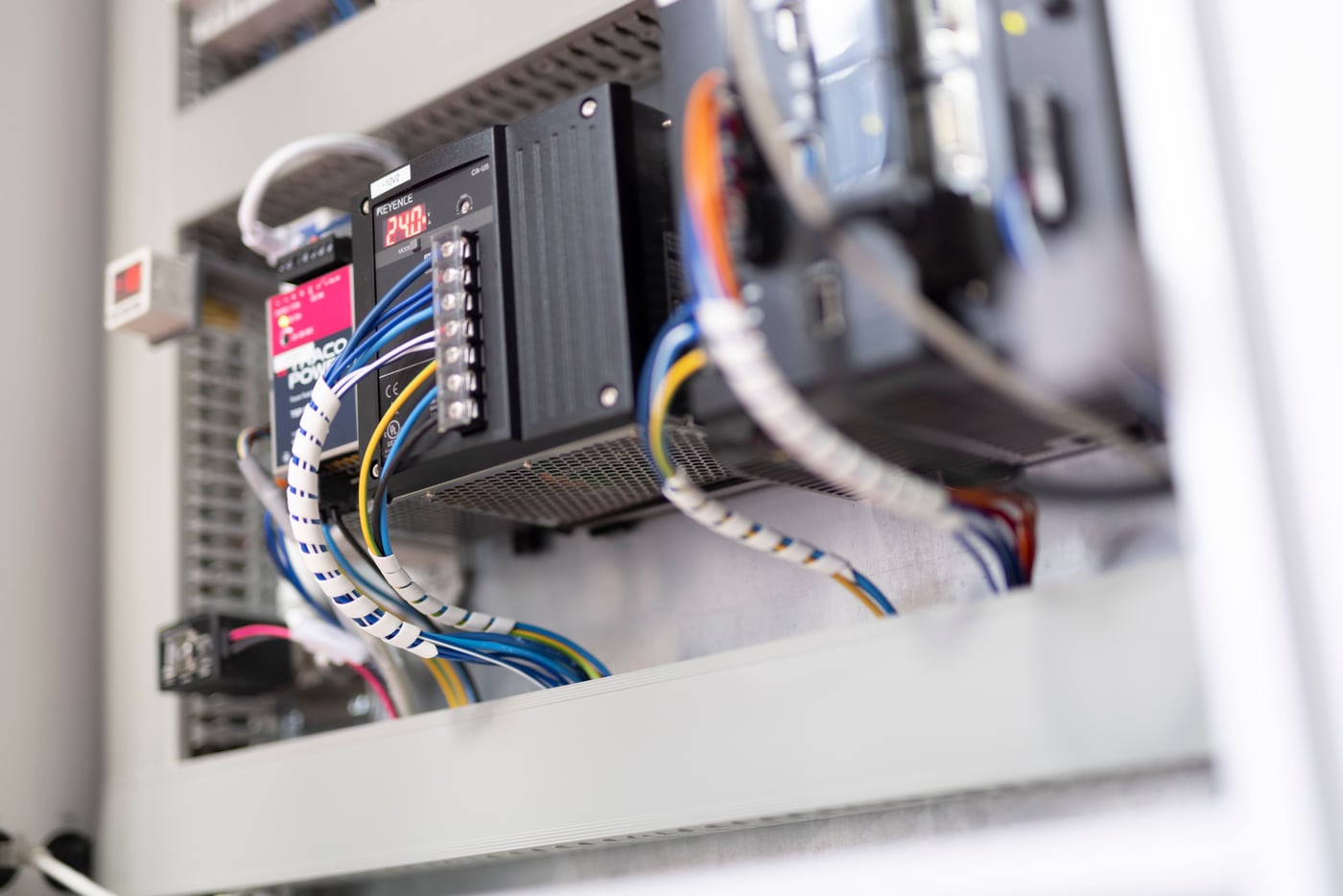
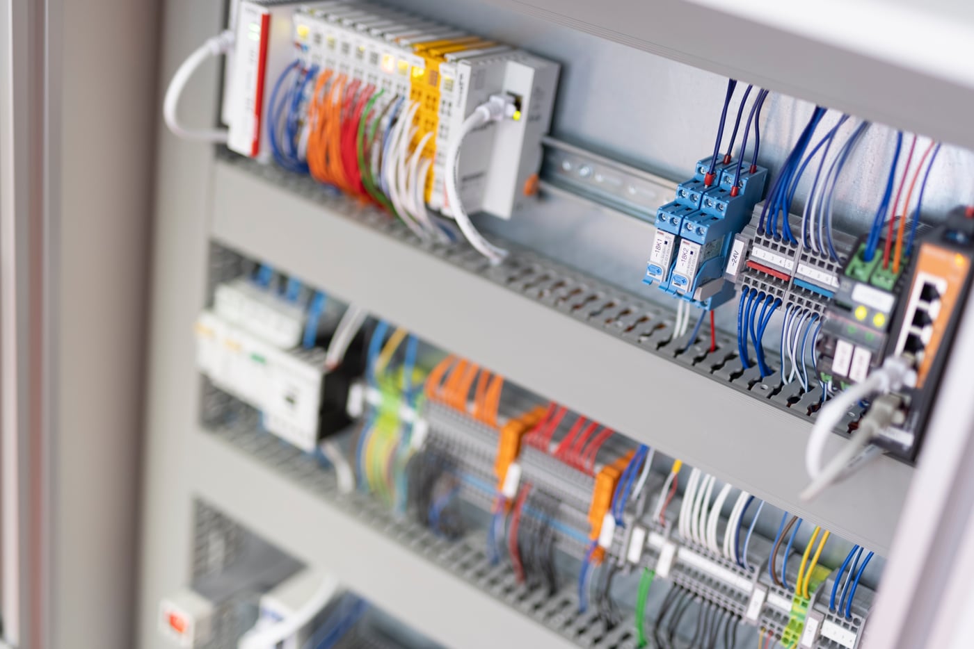
Everything is controlled by the integrated IPC: recipes with target temperature, ramp and hold times, real-time chart monitoring and data export. Every test is traceably documented for every single wafer. And Helios slots seamlessly into the fab, through Ethernet, EtherCAT, SECS, API, FDC and digital I/O.
And because a fab never stands still, neither does Helios: round-the-clock duty in cleanrooms up to and including ISO 5, a redundant architecture, UPS backup for the entire system and a safety-interlocked door. Inspection at the pace of production, day and night.
How the test runs
Fix and heat
The wafer is held on the hot plate by vacuum and brought to target temperature by recipe, with defined ramp and hold times.
Illuminate and capture
The dome light projects a line pattern onto the wafer; the camera captures a series of images while the linear axis moves it step by step.
Analyse and document
The analysis detects cracks and damage in the images and documents the result traceably for every wafer.